
Nano-Scale “Gentle Force” Reshapes Precision Optical and Compound Semiconductor Polishing
Colloidal Silica Advances CMP Technology for InP Wafers and High-End Optical Components
Colloidal Silica Brings Chemical-Mechanical Precision to Advanced Polishing
In the pursuit of optical perfection, precise refractive-index control and lossless light transmission depend heavily on atomically smooth substrate surfaces. From high-end camera lenses to indium phosphide (InP) wafers used in optical communications, polishing has evolved far beyond simply leveling a surface. It has become a microscopic process involving the coordinated action of chemistry and mechanics.
In this precision-manufacturing environment, colloidal silica is reshaping optical processing through its unique nanoscale dispersion system and its comparatively gentle polishing action.
From “Hard Grinding” to “Gentle Polishing”
Traditional optical polishing often relies on hard abrasives. Although these materials can remove stock rapidly, they may also leave micro-scratches or subsurface damage layers on the substrate—defects that can seriously compromise high-precision optical components.
The introduction of colloidal silica slurries marks a transition from conventional polishing to chemical mechanical planarization (CMP).
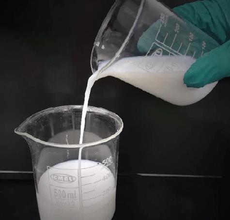
Colloidal silica consists of stable, nanoscale silicon dioxide particles dispersed in water. During polishing, the particles do not rely solely on mechanical hardness to remove material. Instead, surface silanol groups—Si-OH—interact with the optical material through relatively mild chemical adsorption and reactions, forming an extremely thin softened layer.
Mechanical friction from the polishing pad then gently removes this softened material. This combined mechanism of chemical softening and mechanical micro-cutting can significantly reduce surface roughness while minimizing lattice damage caused by excessive mechanical stress.
Tackling Compound Semiconductor Polishing Challenges
Compound semiconductor materials such as lithium phosphate (Li₃PO₄) and indium phosphide (InP) have attracted significant attention in optoelectronics and semiconductor applications because of their strong optical and electrical properties. However, their polishing requirements are also substantially more demanding.
Indium Phosphide Wafers
InP is a key substrate material for optical communications and laser devices. It is relatively soft and chemically reactive, making it vulnerable to surface defects during conventional polishing. Excessive polishing can cause phosphorus loss, resulting in indium-rich regions or pitting.
Colloidal silica optimized for InP can regulate pH and oxidizer ratios with precision. This allows manufacturers to achieve an effective material-removal rate while suppressing selective corrosion. The result is improved control of the wafer’s surface stoichiometry and a higher-quality interface for subsequent epitaxial growth.
Lithium phosphate crystals are used in applications including solid-state electrolytes and optical windows, where surface cleanliness and flatness are critical. The high dispersibility and chemical inertness of colloidal silica enable the slurry to reach microscopic grooves and support global planarization.
At the same time, the process helps avoid metal-ion contamination, supporting the optical and electrical stability of the crystals under demanding operating conditions.
Defining “Polishing-Grade” Colloidal Silica Through Technology
In precision optical and compound semiconductor polishing, purity and particle-size distribution can determine the difference between a successful process and a defective one. Changsha Kona Fine Chemical Co., Ltd., which specializes in fine chemical materials, says customers require more than a container of polishing slurry—they need a stable and complete surface-processing solution.
Extremely Narrow Particle-Size Distribution
The company’s optical-grade colloidal silica is designed with strict control over large-particle counts, or LPCs, to maintain nanoscale particle monodispersity. During polishing, this produces a more uniform cutting force and helps prevent orange-peel textures and deep scratches.
System Stability
Compound semiconductor polishing involves complex chemical conditions. Colloidal silica must therefore offer strong resistance to agglomeration and sedimentation. Even during extended recirculating operations or high-solids processing, a stable colloidal system can reduce the frequency of equipment cleaning and improve production-line yield.
Customized Formulation Capability
From high-end optical lenses to compound semiconductors such as InP and gallium arsenide (GaAs), materials vary widely in hardness and chemical-bond strength. Customized slurry formulations are therefore essential for balancing removal rate, surface quality, defect control, and process stability.
The flatness of an optical wafer forms the information foundation of the optical communications era, while a flawless lens serves as the visual core of precision instruments. As manufacturing moves toward atomic-scale precision, Changsha Kona Fine Chemical aims to provide stable nanoscale abrasives, backed by specialized technical expertise and stringent quality standards, for demanding precision-polishing applications.



 | Address: |
 | Call Us: |
 | Email: inquiry@polishingslurry.com |
